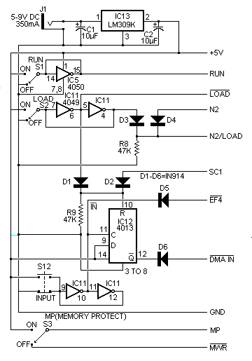
Fig. 5. Control circuits for the computer. Connections at right go to similarly marked connections on main circuit.
Note that each machine cycle requires eight clock pulses.
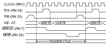
The microprocessor has an internal single-phase clock circuit. Connecting a crystal between pins 1 and 39 of the 1802 chip causes the clock to run continuously. If desired, XTAL, C3, C4, and R11 can be omitted and an external clock with a 5-volt swing can be substituted between pin 1 and ground.
During each machine cycle, timing pulses TPA and TPB are available at pins 33 and 34 of the 1802. TPA occurs at the beginning of each machine cycle and can be used to clock the high-order byte of a 16-bit memory address into a memory page-selection register. Note that the 1802 sends out memory addresses as two 8-bit bytes. The high-order byte appears on address lines A0 through A7 first. Then the low-order byte is held on the A0 through A7 lines for the remainder of the machine cycle. This low-order address byte can, by itself, specify one of 256 locations in the minimum 256-byte memory.
TPB occurs toward the end of the machine cycle and is used to clock a byte from the RAM into an output device (such as the hex display used here). An input byte, to be stored in the RAM, is gated to the bus for the duration of the input (memory-write) machine cycle so that no time pulse is needed for input bytes.
The ~MREAD line is low during any memory-read machine cycle. When low, it opens the pin-18 RAM data output gates of IC2 and IC3, permitting the byte stored in the RAM location addressed by A0 through A7 to appear on the data bus. The RAM's access time is such that the output byte appears on the bus prior to TPB. The bus byte from the RAM can then be clocked into an internal register of the 1802 or clocked to an external register (such as the hex display) with TPB, depending on the type of instruction being executed.
[Note: The ~MREAD above has a line over the MREAD instead of using the tilde, in the article. However, there isn't any HTML tag to put a line over characters, so I'm using the tilde convention instead. The overhead line, or tilde represent active-low signals.]
When the 1802 is performing an instruction cycle that requires a byte to be stored in the RAM, the ~MREAD line is held high to disable the RAM output bus gates. The microprocessor then causes the byte stored in the RAM to be gated onto the bus during the memory-write cycle. This byte can come from an internal register of the 1802 or from an input device such as switches, depending on the type of instruction being executed. The 1802 then generates a low memory-write pulse (~MWR) that causes the bus byte to be stored in the RAM location addressed by the A0 through A7 lines.
Circuit Operation. Using Fig.4, Fig.5, and the Instruction Subset Table we can now discuss the logic of the Elf microcomputer. The RAM access is sent out on lines A0 through A7. Eight tri-state bidirectional bus lines are used to transfer the data bytes back and forth between the 1802's registers and the IC2-IC3 RAM. A RAM byte can be transferred to hex displays IC6 and IC7 via the data bus using IC4 and IC5 to supply the current drive for the displays. Displays IC6 and IC7 contain latches to store the display byte.
The basic clock frequency of the processor is determined by XTAL which should not go above 2 MHz in this circuit. The ~MREAD and ~MWR lines control the read and write cycles of the RAM, while TPA and TPB provide the timing pulses. TPA can be used for memory expansion address latching. TPB to clock bytes into output circuits. SC0 and SC1 indicate the type of cycle being performed by the 1802.
The N0, N1, and N2 lines are used to select input or output devices in the Elf, selection can be made among four input and four output devices. The table details the values of the N0, N1, and N2 lines during the machine cycle in which an input or output instruction is executed. Instructions 69, 6A, 6B, 61, 62, and 63 are spares that can be used to add I/O devices or ports to the computer. When 6C is executed, the N2 line goes to a logic-1 state and the bus byte is written into the RAM. Since this is a write cycle, ~MREAD will be high. With both N2 and ~MREAD high, the output of gate IC10C will be low, putting the input toggle switch byte on
[33] [34] [35] [36] [37] [38]